In technology-driven industries, understanding a material’s structure, composition, and defects at the microscopic level is essential. Whether it’s for failure investigation, quality control, or research and development, precision matters. This is where the Scanning Electron Microscope (SEM) with EDS Analysis comes into play.
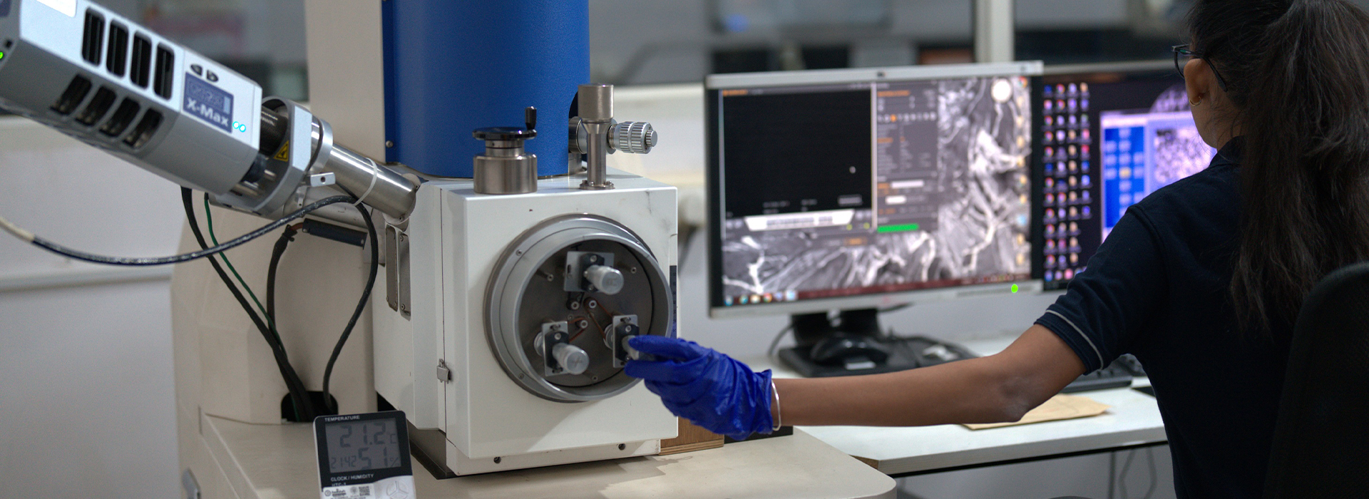
At TCR Advanced Engineering, we offer state-of-the-art Scanning Electron Microscopy (SEM) and Energy Dispersive Spectroscopy (EDS) analysis services to help you uncover the microscopic details of your materials. We are among the India’s few private Laboratory to have 3 Electron Microscopes in the laboratory premises. Our advanced SEM models, Pemtron SS100, Jeol JCM 6000+ and Phenom XL G2, are equipped with cutting-edge features to provide precise and reliable results.
— delivering results that save time, money, and resources.
What is SEM-EDS Analysis?
SEM-EDS Analysis is a two-part process combining Scanning Electron Microscopy (SEM) with Energy Dispersive X-ray Spectroscopy (EDS).
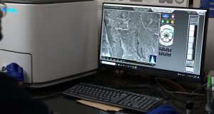
– Scanning Electron Microscopy (SEM) allows scientists and engineers to take extremely high-resolution images of a material’s surface. It uses a focused beam of electrons instead of light to magnify the sample up to hundreds of thousands of times.
– Energy Dispersive X-ray Spectroscopy (EDS), also known as SEM-EDX Analysis, detects and measures the X-rays emitted from the sample when it is hit by the electron beam. This reveals the chemical composition of the material.
When combined, EDS Analysis with SEM provides both the surface structure and the elemental composition of a sample, making it one of the most powerful tools for material characterization.
 Key Features of Our SEM equipments
Jeol JCM 6000+
The Jeol JCM 6000+ is a versatile benchtop SEM that offers:
- High Resolution: Achieve up to 60,000X magnification with high sensitivity backscatter electron detection.
- Intuitive Operation: Easy-to-use touch panel interface with advanced automatic functions for focus, stigmation, brightness, and contrast.
- Quick Response: Images can be displayed within 3 minutes of starting the instrument.
- Dual Vacuum Modes: High and low vacuum modes for flexible sample imaging.
- Elemental Analysis: Optional EDS installation for qualitative and quantitative analysis.
- Elemental Mapping
- Phenom XL G2
- The Phenom XL G2 is a desktop SEM designed for high-throughput analysis:
- Large Sample Stage: Accommodates samples up to 100 x 100 mm.
- Fast Imaging: Average time-to-image of just 60 seconds.
- Long Lifetime Source: Unique Cerium Hexaboride (CeB6) electron source for less maintenance.
- Automation: Automates repetitive tasks and quality control processes.
- Environmental Compatibility: Can be placed in a dry room or argon glove box for reactive sample research.
- What is SEM-EDS Used For?
SEM/EDS Analysis for Material is used across multiple industries to:
Applications of SEM
1.Fracture Analysis: Identifying the mode of fracture (ductile, brittle, fatigue) and determining the origin of fractures.
2.Surface Topography: Examining surface features, textures, and morphology of materials.
3.Grain Size and Shape Analysis: Analyzing the size, shape, and distribution of grains in metallic samples.
4.Corrosion Studies: Investigating corrosion mechanisms and identifying corrosion products on metal surfaces.
5.Failure Analysis: Determining the root cause of material failures by examining microstructural defects.
6.Wear Analysis: Studying wear patterns and mechanisms on metal surfaces.
7.Material Characterization: Identifying phases, inclusions, and other microstructural features.
Applications of EDS
1.Elemental Composition Analysis: Identifying and quantifying the elemental composition of materials.
2.Contaminant Detection: Detecting and analyzing contaminants and impurities in metals.
3.Coating Analysis: Evaluating the thickness and composition of coatings on metal surfaces.
4.Corrosion Analysis: Identifying elements involved in corrosion processes and mapping their distribution.
5.Phase Identification: Determining the phases present in a material and their distribution.
6.Inclusion Analysis: Detecting and quantifying trace elements in metallic samples.
7.Phase Identification : microscopic level analysis if Phase identification is possible with EDS analysis
8.Material Identification of miniature components :
9.Elemental Mapping : possible to do elemental mapping to visualise the homogeneity and uniformity of alloy distribution
10.Coating Identification : can identify multi layer coatings.
This combination of Scanning Electron Microscopy (SEM) and energy dispersive X-ray spectroscopy (EDS) enables engineers to see the smallest details while understanding exactly what elements are present.
How Does SEM-EDS Work?
The working principle is simple yet powerful:
1. A focused electron beam scans the surface of the sample inside the SEM chamber.
2. When electrons hit the material, they interact with atoms, releasing various signals — including X-rays.
3. The EDS detector measures these X-rays, as each element emits X-rays with unique energy levels.
4. The system then produces both high-resolution images and elemental composition maps.
With EDX Analysis with SEM, you get a complete picture: what the material looks like, and what it’s made of.
 Why SEM-EDS Analysis is Important
In manufacturing and engineering, small defects can lead to big problems — equipment failures, safety hazards, or costly recalls. SEM/EDS Analysis for Material helps detect issues before they become critical. It is essential for:
1. Failure Investigation
SEM/EDS Analysis for Material allows engineers to examine fractures, corrosion, and defects at the microscopic level. By identifying the root cause of a failure, industries can prevent similar issues in the future. This leads to safer and more reliable products.
2. Quality Control
Using a Scanning Electron Microscope (SEM) with EDS Analysis ensures materials match the exact specifications required for production. Even the smallest impurities or inconsistencies can be detected before products leave the factory. This reduces rework, waste, and customer complaints.
3. Research & Development
In product innovation, understanding material properties at the micro and nano scale is critical. SEM/EDX Analysis provides detailed data to improve designs, choose better materials, and test new concepts. This accelerates development without compromising on quality.
4. Regulatory Compliance
Many industries must follow strict material composition and safety standards. EDS Analysis with SEM verifies that products meet these legal and quality requirements. This helps companies avoid penalties, recalls, and damage to their reputation.
By combining Scanning Electron Microscopy with EDS, industries can solve problems with unmatched precision.
Benefits for Different Industries
1. Power Generation Industry
In power plants, even microscopic cracks or corrosion can cause massive breakdowns. SEM-EDS Analysis helps detect wear, creep, and corrosion in turbine blades, boilers, and other critical components before failure occurs.
2. Fertilizer Industry
Corrosion and contamination can impact production efficiency. Scanning Electron Microscopy (SEM) with energy dispersive X-ray spectroscopy (EDS) helps identify contaminants in a corrosive environment and improve material durability.
3. Chemical and Petrochemical Industry
Pipes, reactors, and storage tanks face harsh chemical environments. SEM-EDX Analysis can reveal corrosion products and help select better materials for long-term performance.
4. Oil & Gas
In this high-risk sector, EDS Analysis with SEM detects microscopic defects in drilling tools, pipelines, and subsea equipment — improving safety and reliability.
5. Insurance Sector
When equipment fails, insurance investigations rely on failure analysis. SEM/EDS Analysis for Material provides undeniable evidence of cause and responsibility.
6. Engineering Procurement and Construction (EPC)
For EPC companies, SEM-EDS Analysis ensures that materials used in projects meet exact specifications, preventing costly rework.
7. Pharmaceutical Industry
Contamination in medicines can have serious consequences. Scanning Electron Microscope (SEM) with EDS Analysis identifies foreign particles and ensures product purity.
8. Fabrication Industry
Welds and joints are inspected using SEM-EDX Analysis to guarantee structural strength and quality by evaluating microstructure of materials, Weld and harmful phases compromising the quality of materials
9. Manufacturing Industry
From automotive parts to electronic devices, EDS Analysis with SEM helps maintain consistent product quality and detect defects early.
10. Automobile Industry
In cars, tiny material defects can cause long-term performance issues. Scanning electron microscopy with EDS identifies problems during production and after failures.
Why Choose TCR for SEM-EDS Analysis?
At TCR Advanced, we are equipped with the latest Scanning Electron Microscope (SEM) and advanced EDS Analyzer technology.
Our SEM and EDS analysis services are ideal for a wide range of applications, including failure investigation, quality control, corrosion analysis, and material characterization. With TCR Advanced Engineering, you can trust in precision, transparency, and reliability for all your testing needs.
Discover the microscopic world with us and elevate your material analysis to the next level!
1. Failure Investigation
This process involves finding out why a material or component broke, cracked, or stopped working. Using SEM-EDS, experts can examine microscopic features to detect manufacturing defects, stress damage, or environmental factors that caused the failure.
2. Fractography
Fractography is the study of fracture surfaces on broken parts. SEM provides high-resolution images that reveal patterns like brittle fracture, fatigue, or ductile tearing. This helps engineers understand how and where the break started.
3. Morphology Analysis
Morphology analysis looks at the shape, structure, and texture of a material’s surface. SEM magnifies the surface thousands of times, making it possible to see roughness, cracks, or patterns invisible to the naked eye.
4. Corrosion Product Identification
When metal corrodes, it leaves behind deposits or rust-like products. EDS analysis determines the exact chemical composition of these corrosion products, helping to identify the cause — whether it’s due to moisture, chemicals, or environmental exposure.
5. Surface Coating Verification
This process checks if protective coatings (like paint, plating, or film) are applied correctly and are uniform. SEM/EDS can detect coating thickness, adhesion quality, and any unwanted gaps or contamination.
6. Particle Size & Shape Analysis
SEM can measure and analyze microscopic particles in a material. By studying their size and shape, industries can ensure materials meet required specifications for performance, safety, or appearance.
7. Creep Detection
Creep is the slow, permanent deformation of a material when it’s under stress for a long time, often at high temperatures. SEM can detect early signs of creep damage before it leads to complete failure.
8. Inclusion Identification
Inclusions are tiny unwanted materials trapped inside metals or alloys during manufacturing. SEM/EDS identifies their size, shape, and composition, which helps prevent weakness or defects in the final product.
Our expert team ensures that every analysis delivers actionable insights you can trust.
FAQs
Q1. What is the main advantage of SEM over traditional microscopes?
Traditional microscopes only provide visual images, while SEM-EDS Analysis offers both structural and elemental composition data, making it much more powerful.
Q2. How long does a typical SEM/EDS Analysis take?
Depending on the sample size and complexity, analysis can take from 30 minutes to a few hours. TCR ensures quick turnaround without compromising accuracy.
Q3. Can SEM Analysis detect very small particles?
Yes, our system can detect particles at submicron levels, ensuring no defect or contaminant goes unnoticed.
Q4. Is EDS Analysis with SEM destructive to the sample?
Generally, the process is non-destructive, meaning your sample remains intact after analysis but SEM sample chamber has limited size hence bigger samples need to be tested by cutting a smaller piece.
Q5. Which industries benefit most from SEM/EDS Analysis for Materials?
Industries such as power generation, oil & gas, manufacturing, pharmaceuticals, and automotive rely heavily on this technology for quality control and problem-solving.
Q6. Can SEM-EDS Analysis detect submicron features in materials?
Yes, Scanning Electron Microscopy (SEM) with EDS Analysis can detect features smaller than a micron, allowing detailed observation of microstructures, inclusions, and defects that are invisible to standard microscopes.
Q8. How accurate is the elemental composition measured by EDS Analysis with SEM?
The EDS Analyzer with SEM provides highly accurate elemental identification and quantification, However EDS analysis is not suitable for trace level analysis typically less than 0.1 % concentration .
Q9. Can SEM/EDS Analysis be used for all types of materials?
Yes, SEM-EDS Analysis for Material works with metals, ceramics, polymers, composites, and even biological samples, making it versatile across industries like manufacturing, pharmaceuticals, and petrochemicals.
Q10. How does SEM/EDS help in preventive maintenance?
By identifying early signs of wear, corrosion, or microstructural changes, Scanning Electron Microscopy (SEM) with EDS Analysis allows industries to take corrective actions before major failures, improving safety and reducing maintenance costs.
Final Thoughts
The Scanning Electron Microscope (SEM) with EDS Analysis is more than just a testing method — it’s a decision-making tool for industries where precision, safety, and reliability are critical. Whether you’re troubleshooting a failure, developing a new product, or ensuring compliance with standards, SEM/EDS Analysis for Materials gives you the confidence that comes from knowing your materials inside and out.
At TCR Advanced, our combination of cutting-edge technology and experienced professionals ensures you get accurate, reliable, and timely results every time.


